경제적이고 확장 가능한 통합 광학 및 어레이 장비 제조
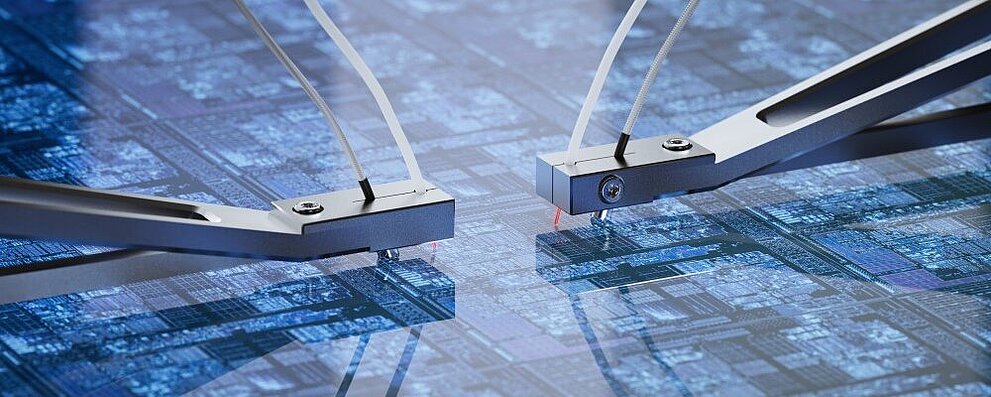
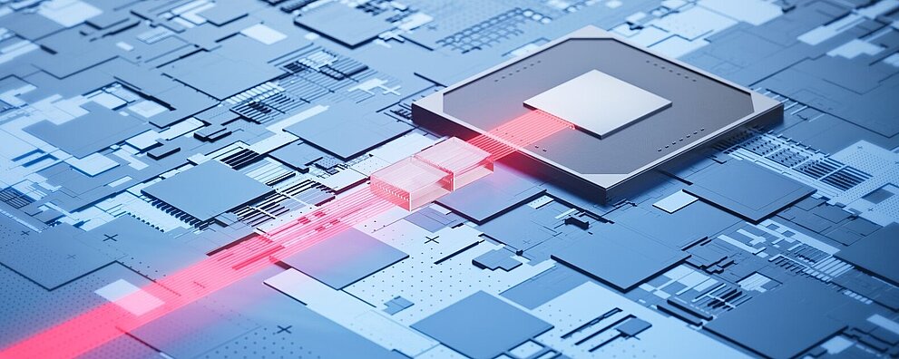
낮은 에너지 소비로 막대한 전송 용량을 제공하는 광학 통신은 통신 네트워크의 원동력입니다. 실리콘 및 기타 기판의 웨이퍼에 광학 부품을 배치하고 광학 연결을 만드는 것은 실리콘 포토닉스 부품 및 광 집적 회로(PIC)의 생산 및 품질 보증에서 반복되는 공정 단계입니다. 매우 엄격한 횡방향 공차가 요구되는 경우가 많기 때문에 구성품 및 PIC 제조의 기능과 비용 측면에서 정밀도, 속도, 고도의 얼라인먼트 자동화가 필수적인 경우가 많습니다.
PIC 생산에서 주요 비용 요인 제거
웨이퍼 수준부터 조립, 패키징에 이르는 실리콘 포토닉스(SiPh) 장비 제조에서 얼라인먼트 시간은 주요 비용 요인입니다. 웨이퍼 수준 테스트의 경우, 이는 엔지니어링 프로버에 적용되며 가동 시간과 처리량이 특히 중요한 생산 프로버에는 더욱 그렇습니다. 고급 자율 얼라인먼트 기능과 반도체 공장 인증 메커니즘을 갖춘 PI의 포토닉스 얼라인먼트 알고리즘 및 하위 시스템은 기존 얼라인먼트 기술에 비해 몇 배나 향상된 속도, 처리량, 정확도를 제공하여 업계의 까다로운 요구 사항을 충족합니다. 광학 패키징에서는 광섬유, 도파관 및 기타 구성품의 얼라인먼트를 세심하게 제어해야 합니다. PI는 어레이 얼라인먼트에 대한 전문성을 바탕으로 실리콘 포토닉스 애플리케이션의 엄격한 요구 사항을 충족하는 솔루션을 제공할 수 있습니다. 고급 위치 제어 시스템과 얼라인먼트 알고리즘을 활용하여 뛰어난 성능과 안정성을 구현합니다.
까다로운 실리콘 포토닉스 애플리케이션을 위한 통합 솔루션
웨이퍼 수준의 광학 장비 및 구성품 품질 보증부터 칩 테스트, 최종 조립 및 패키징에 이르기까지 PI는 다양한 칩 설계, 형식 및 작업을 위한 포괄적이고 다양한 솔루션을 제공합니다.
파트너로서 PI의 장점
- 첨단 기술을 사용하여 포토닉스 얼라인먼트 공정의 속도와 정확성을 향상하도록 설계된 모션 제어 시스템
- PI 모션 제어 및 얼라인먼트 알고리즘은 First Light를 찾고, 커플링을 특성화하고, 여러 입력과 출력을 동시에 정렬하기 위한 고유한 방법 제공
- 고객과의 긴밀한 협업을 통해 고객의 고유한 요구 사항을 파악하고 고객의 구체적인 요구 사항을 충족하는 맞춤형 솔루션 제공
- 모션 제어 시스템 및 포토닉스 얼라인먼트 솔루션 개발 및 구현 분야에서 수십 년의 경험을 보유한 전문가 팀
- 북미, 아시아, 유럽에 위치한 설계, 생산, 서비스 센터를 통해 다음 프로젝트를 가속화 가능